INSTRUMENTATION
Scanning Tunneling Microscopy (STM)
Launch: 16 Mar 2026, 05:00 PM
One Day Online Instrumentation program on Scanning Tunneling Microscopy (STM)
Workshop Highlights
Introduction and History of STM
Basics and evolution of Scanning Tunneling Microscopy
Development in surface physics and nanotechnology
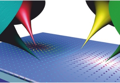
Principle of STM
Quantum tunneling effect
Tunneling current between conductive tip and sample
Imaging Modes
Constant current mode
Constant height mode
Sample Preparation Techniques
Clean conductive surfaces
Ultra-high vacuum conditions
Case Study
Atomic-resolution imaging of metal surfaces
Applications and Examples
Surface science
Nanotechnology
Semiconductor research
Program Particulars
| Particulars | Details |
|---|
| Title | Scanning Tunneling Microscopy (STM) |
| Duration | 1 hour |
| Mode of Delivery | Online session |
| Program Fee | ₹149 (Individual Registration) |
| Deliverables | E-Certificate, Course Material |
| Target Audience | Students, Researchers, Professionals in Nanotechnology, Physics, Materials Science |
- ✓ Understand quantum tunneling principles for atomic-level imaging.
- ✓ Analyze conductive surface structures at atomic resolution
Mrs.Nandhini Muthukumaran
Nanotechnologist
Founder and Director of Nano Nest Private Limited
Excels in the fabrication of nanoparticles
Expertise in characterization of nanomaterials
Skilled in curating scientific and technical workshops
Delivers complex concepts in a clear and understandable manner
Experienced in hands-on training and practical demonstrations
Strong ability to engage students, researchers, and professionals
Focused on industry-relevant and application-oriented learning